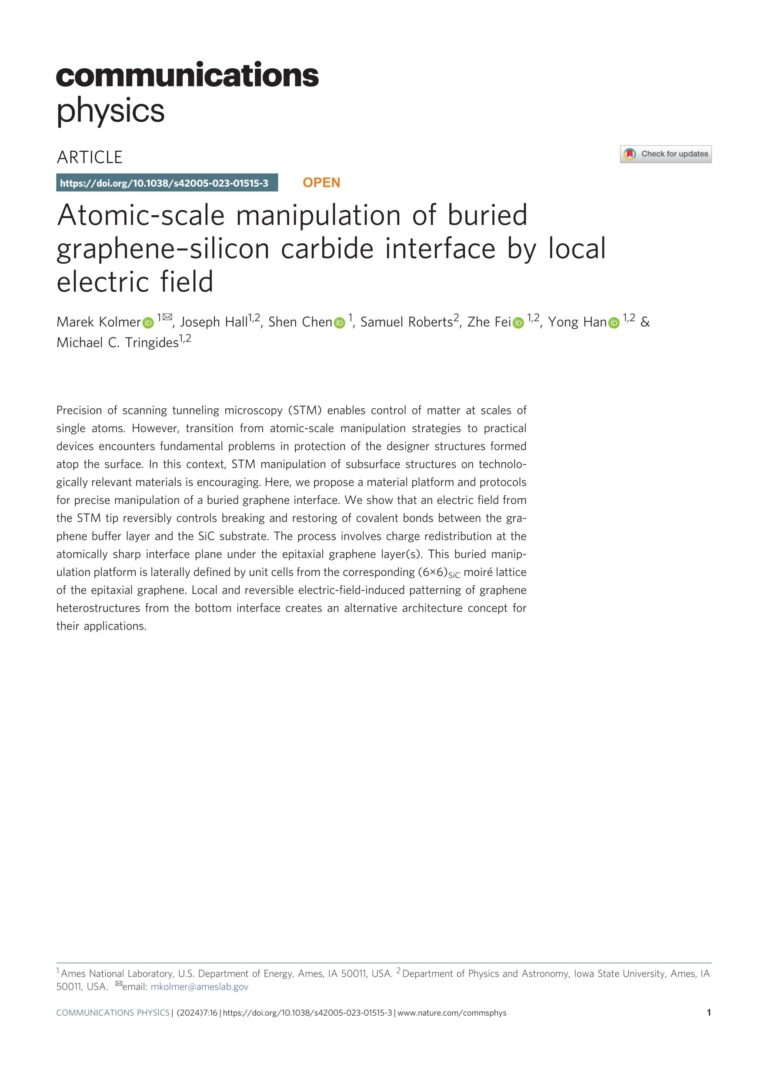
In 2024 one of our clients published the first scientific paper using our graphene.
Below you can find an abstract of the article and a full downloadable text in pdf.
Abstract
Precision of scanning tunneling microscopy (STM) enables control of matter at scales of single atoms. However, transition from atomic-scale manipulation strategies to practical devices encounters fundamental problems in protection of the designer structures formed atop the surface. In this context, STM manipulation of subsurface structures on technologically relevant materials is encouraging. Here, we propose a material platform and protocols for precise manipulation of a buried graphene interface. We show that an electric field from the STM tip reversibly controls breaking and restoring of covalent bonds between the graphene buffer layer and the SiC substrate. The process involves charge redistribution at the atomically sharp interface plane under the epitaxial graphene layer(s). This buried manipulation platform is laterally defined by unit cells from the corresponding (6×6)SiC moiré lattice of the epitaxial graphene. Local and reversible electric-field-induced patterning of graphene heterostructures from the bottom interface creates an alternative architecture concept for their applications.


